BeSANG Developed High Density Vertical Flash Memory

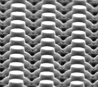
A close-up view of the vertical memory cells
The vertical flash memory cell is based on well-known SGT technology and uses single crystalline silicon material. Conventional CMOS tools, materials, and CMOS processes are used to implement the high density vertical flash memory, providing an added advantage.
"BeSang's 3D technology is very significance because it is a novel combination of well-known CMOS process and device technologies. Many other emerging technologies were not successful in commercialization because they were based on new materials and new device concepts and CMOS fabs have little accumulated experience in manufacturing these emerging technologies. Hence, conventional CMOS technology has prevailed in the market for decades even though advanced CMOS technology is becoming less and less affordable," said Dieter K. Schroder, Professor at Arizona State University.
Conventional 3D chip technologies are merely package-level multi-chip stacking technologies with limited mobile applications. The technology developed by BeSang allows vertical memory cells to be stacked on top of conventional CMOS logic within a semiconductor chip, using seamless and unlimited interconnects between device layers. As a result, this single-chip, high-density 3D technology provides the semiconductor industry with a low-cost, high-performance vertical memory solution.
About BeSang
BeSang is a fabless semiconductor IP company providing its proprietary 3D Enabling Technology. The Company is entering the semiconductor memory business for both stand-alone and embedded memory markets. The main mission of the Company is to provide unique “Single-Chip 3D” enabling solutions that can significantly reduce die cost of semiconductor chips, including ultra high density memories and high quantum efficiency image sensors. BeSang has developed high value intellectual property related to its single-chip 3D Enabling Technology. This technology will be important for companies in the stand-alone, microprocessor, system-on-a-chip (SoC), and image sensor markets. For more information, see BeSang’s Website at http://www.BeSang.com
BeSang Inc 개요
BeSang은 재미 한인 과학 기술자들이 주축이되어, 미국 포틀렌드 오레곤에 설립된 펩리스 반도체 벤처 회사이며, 새로운 3차원 반도체 기술과 지적 재산을 제공하고 있다. BeSang의 3차원 반도체 기술은, 로직을 구성하는 일반 CMOS 웨이퍼 위에 메모리나 이미지 센서등을 형성하는 단결정 실리콘 층을 연속적으로 형성하는 기술이다. BeSang은 본 3차원 반도체에 관련된 원천 기술을 보유하고있으며, 본 기술을 고객인 반도체 제조 회사들에게 제공하여, 하나의 웨이퍼에서 2배에서 5배까지 많은 칩을 생산하여, 생산 원가를 줄이고, 고 부가 가치의 제품을 만들수 있도록 돕는 역활을 한다.
웹사이트: http://www.besang.com
연락처
Sang-Yun Lee
President and CEO, BeSang
(Phone) 503-533-5150 (Cell) 503-502-3366
(E-mail) 이메일 보내기
