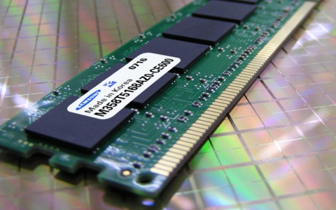
Samsung Electronics Develops New, Highly Efficient Stacking Process for DRAM

“The innovative TSV-based MCP (multi-chip package) stacking technology offers next-generation packaging solution that will accommodate the ever-growing demand for smaller-sized, high-speed, high-density memory,” said Tae-Gyeong Chung, vice president, Interconnect Technology Development Team, Memory Division, Samsung Electronics. “In addition, the performance advancements achieved by our WSP technology can be utilized in many diverse combinations of semiconductor packaging, such as system-in-package solutions that combine logic with memory.
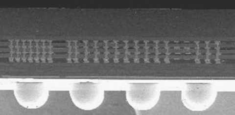
In today’s MCPs, memory chips are connected by wire bonding, requiring vertical spacing between dies that is tens of microns deep. That wire bonding process also requires horizontal spacing on the package board hundreds of microns wide for the die-connecting wires. By contrast, Samsung’s WSP technology forms laser-cut micron-sized holes that penetrate the silicon vertically to connect the memory circuits directly with a copper (Cu) filling, eliminating the need for gaps of extra space and wires protruding beyond the sides of the dies. These advantages permit Samsung’s WSP to offer a significantly smaller footprint and thinner package.
Inside the new WSP, the TSV is housed within an aluminum (Al) pad to escape the performance-slow-down effect caused by the redistribution layer. Due to the complexity of DRAM stacking, this represented a much more difficult engineering feat than that accomplished with the first WSP, announced last year involving NAND flash dies.
There has been considerable concern that MCPs with high-speed memory chips with speed of 1.6Gb/ps next generation DRAM, would suffer from performance limitations when connected using current technologies. Samsung’s WSP technology resolves these concerns.
In addition, as the back side of the wafer is ground away to make a thinner stack of multiple dies, the wafer has had a tendency to curve, creating physical distortion in the die. To overcome this additional critical concern in designing low-profile, high-density MCPs containing DRAM circuitry, Samsung’s proprietary wafer-thinning technology, announced last year, has been applied to improve the thin-die-cutting process.
Advanced package solutions are increasingly important requirements for enabling high-speed, high-density memory solutions. Samsung’s new stacked package design supports the rapid industry demand for high density, high performance semiconductor solutions that will support next-generation computing systems in 2010 and beyond.
About Samsung Electronics
Samsung Electronics Co., Ltd. is a global leader in semiconductor, telecommunication, digital media and digital convergence technologies with 2006 parent company sales of US$63.4 billion and net income of US$8.5 billion. Employing approximately 138,000 people in 124 offices in 56 countries, the company consists of five main business units: Digital Media Business, LCD Business, Semiconductor Business, Telecommunication Network Business, and Digital Appliance Business. Recognized as one of the fastest growing global brands, Samsung Electronics is a leading producer of digital TVs, memory chips, mobile phones, and TFT-LCDs. For more information, please visit www.samsung.com
삼성전자 개요
삼성전자는 반도체, 통신, 디지털 미디어와 디지털 컨버전스 기술을 보유한 글로벌 리더다. 삼성전자는 디지털 어플라이언스 부문, 디지털 미디어 부문, LCD 부문, 반도체 부문, 통신 네트워크 부문 등 5개 부문으로 이뤄져 있다. 세계에서 가장 빠르게 성장하는 브랜드인 삼성전자는 스마트폰, 디지털 TV, 메모리 반도체, OLED, TFT-LCD 분야에서 세계 선두 주자다.
웹사이트: http://www.samsung.com/sec
연락처
Suyeon Chae
tel : 82-2-727-7824
email : 이메일 보내기
기자 발굴부터 성과 측정까지 PR 업무 시간을 절반으로

-
6월 26일 13:59
