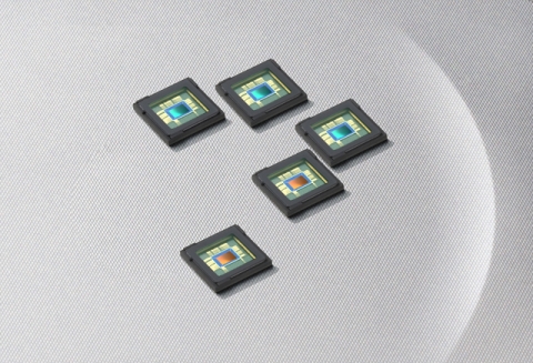
Samsung Develops 12 Megapixel CMOS Imager with 1.12um Back Side Illuminated Pixel Architecture for High–quality Imaging on Premium Feature and Smart Phones
The S5K3L1 supports 12Mp full resolution images at 30 frames per second (fps) and 1080p full HD video at 60fps enabling crisp still photos and high-speed video recording, as well as 720p at 90fps and VGA resolution images at 120fps for slow motion playback function in mobile phones. The new image sensor also includes an on-chip pixel correction feature, compensating color and luminance response variations to address image distortion.
In addition, the 12Mp imager offers an optional RGB-white color filter array, which delivers advanced sensitivity while reducing noise, resulting in a 30 percent brighter image over that of a conventional RGB color filter array. The RGB-white filter feature works in conjunction with a complimentary logic chip (S5C73L1), which converts RGB-White pattern to RGB Bayer for back-end Bayer ISP compatibility. The logic chip also provides features such as lens shading correction, image down scaling, noise reduction and significantly enhanced modulation transfer function to reproduce fine details.
Samsung’s S5K3L1 imager is designed to address an 8.5mm x 8.5mm auto focus camera module with a height dimension of 6.0mm for slim mobile phones and small form factor applications
Samples of the 12Mp imager are available now with mass production scheduled in the third quarter of this year.
The S5K3L1 will be displayed at the Mobile World Congress, Barcelona, Spain from February 14 to 17.
삼성전자 개요
삼성전자는 반도체, 통신, 디지털 미디어와 디지털 컨버전스 기술을 보유한 글로벌 리더다. 삼성전자는 디지털 어플라이언스 부문, 디지털 미디어 부문, LCD 부문, 반도체 부문, 통신 네트워크 부문 등 5개 부문으로 이뤄져 있다. 세계에서 가장 빠르게 성장하는 브랜드인 삼성전자는 스마트폰, 디지털 TV, 메모리 반도체, OLED, TFT-LCD 분야에서 세계 선두 주자다.
웹사이트: http://www.samsung.com/sec
연락처
Jason Kim
Samsung Electronics
+82-2-2255-8276
이메일 보내기
기자 검색부터 배포·모니터링까지 한 곳에서 끝내세요

-
7월 15일 09:44
")